- 您现在的位置:买卖IC网 > Sheet目录1996 > HSP45116AVC-52Z (Intersil)IC OSC NCO 52MHZ 160-MQFP
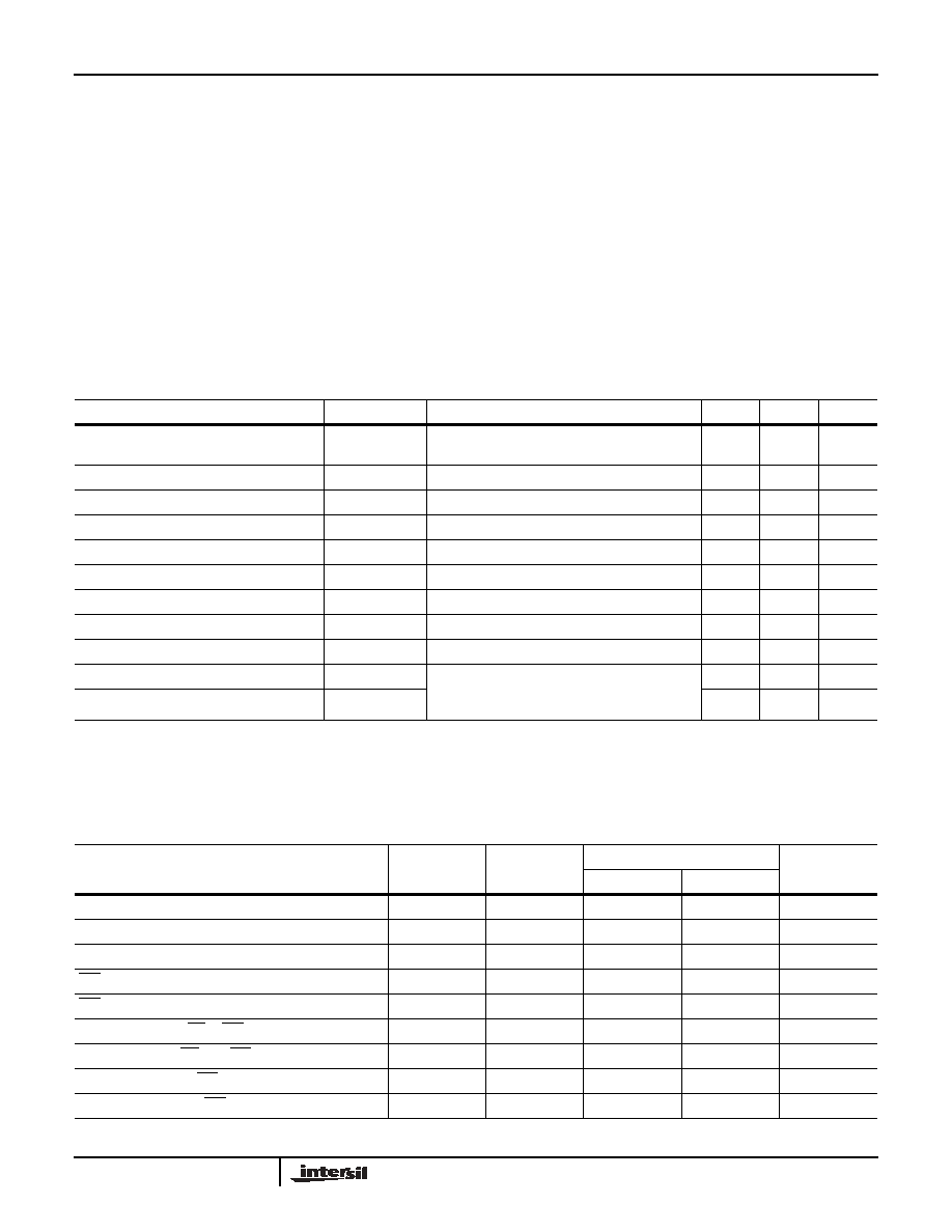
Absolute Maximum Ratings
Thermal Information
Supply Voltage . . . . . . . . . . . . . . . . . . . . . . . . . . . . . . . . . . . . . +7.0V
Input, Output or I/O Voltage Applied . . . . . GND -0.5V to VCC +0.5V
ESD Classification . . . . . . . . . . . . . . . . . . . . . . . . . . . . . . . . . Class 1
Operating Conditions
Voltage Range . . . . . . . . . . . . . . . . . . . . . . . . . . . . +4.75V to +5.25V
Temperature Range . . . . . . . . . . . . . . . . . . . . . . . . . . . 0°C to +70°C
Thermal Resistance (Typical, Note 1)
θJA (°C/W)
MQFP Package . . . . . . . . . . . . . . . . . . . . . . . . . . . .
38.0
Maximum Junction Temperature . . . . . . . . . . . . . . . . . . . . . . +150°C
Maximum Storage Temperature Range . . . . . . . . . . -65°C to +150°C
Pb-free reflow profile . . . . . . . . . . . . . . . . . . . . . . . . . .see link below
Die Characteristics
Gate Count . . . . . . . . . . . . . . . . . . . . . . . . . . . . . . . . . 26,000 Gates
CAUTION: Stresses above those listed in “Absolute Maximum Ratings” may cause permanent damage to the device. This is a stress only rating and operation of the
device at these or any other conditions above those indicated in the operational sections of this specification is not implied.
NOTE:
1.
θ
JA is measured with the component mounted on an evaluation PC board in free air.
15
FN4156.4
May 7, 2007
DC Electrical Specifications
VCC = 5.0V ±5%, TA = 0°C to +70°C
PARAMETER
SYMBOL
TEST CONDITIONS
MIN
MAX
UNITS
Power Supply Current
ICCOP
VCC = Max, CLK Frequency 52.6MHz
Notes 2, 3
-
184
mA
Standby Power Supply Current
ICCSB
VCC = Max, Outputs Not Loaded
-
500
μA
Input Leakage Current
II
VCC = Max, Input = 0V or VCC
-10
10
μA
Output Leakage Current
IO
VCC = Max, Input = 0V or VCC
-10
10
μA
Logical One Input Voltage
VIH
VCC = Max
2.0
-
V
Logical Zero Input Voltage
VIL
VCC = Min
-
0.8
V
Logical One Input Voltage: CLK
VIHC
VCC = Max
3.0
-
V
Logical One Output Voltage
VOH
IOH = -5mA, VCC = Min
2.6
-
V
Logical Zero Output Voltage
VOL
IOL = 5mA, VCC = Min
-
0.4
V
Input Capacitance
CIN
CLK Frequency 1MHz
All measurements referenced to GND.
-
10
pF
Output Capacitance
COUT
-
10
pF
NOTES:
2. Power supply current is proportional to frequency. Typical rating is 3.5mA/MHz.
3. Output load per test circuit and CL = 40pF.
4. Not tested, but characterized at initial design and at major process/design changes.
AC Electrical Specifications
PARAMETER
SYMBOL
NOTES
52.6MHz (-52)
UNITS
MIN
MAX
CLK Period
tCP
19
-
ns
CLK High
tCH
7
-
ns
CLK Low
tCL
7
-
ns
WR Low
tWL
7
-
ns
WR High
tWH
7
-
ns
Setup Time AD0-1, CS to WR
tAWS
10
-
ns
Hold Time AD0-1, CS from WR
tAWH
0
-
ns
Setup Time C0-15 to WR
tCWS
10
-
ns
Hold Time C0-15 from WR
tCWH
0
-
ns
HSP45116A
发布紧急采购,3分钟左右您将得到回复。
相关PDF资料
ICL7109EPL+
IC ADC 12BIT 3-ST 40-DIP
ICM7217AIPI
IC OSC UP/DWN CNTR 2MHZ 28-DIP
ICM7217CIPI
IC OSC UP/DWN CNTR 2MHZ 28-DIP
ICM7242IPA
IC OSC BINARY CTC 13MHZ 8-DIP
ICM7250IWE+T
IC OSC BINARY CTC 15MHZ 16SOIC
ICM7556IPD
IC OSC TIMER DUAL 500KHZ 14-DIP
ICM7556MJD
IC OSC TIMER DUAL 1MHZ 14DIP
ICS180M-03LF
IC CLOCK GEN LOW EMI 8-SOIC
相关代理商/技术参数
HSP45116-DB
制造商:INTERSIL 制造商全称:Intersil Corporation 功能描述:HSP45116 Daughter Board
HSP45116DB-EVAL
功能描述:子卡和OEM板 HSP45116 DAUGHTER EV EVAL BRD
RoHS:否 制造商:BeagleBoard by CircuitCo 产品:BeagleBone LCD4 Boards 用于:BeagleBone - BB-Bone - Open Source Development Kit
HSP45116GC-15
制造商:Rochester Electronics LLC 功能描述:16 BIT NUMERICALLY CONTROLLED OSC/MOD 144 PGA, 15MHZ, COMM - Bulk
HSP45116GC-25
制造商:INTERSIL 制造商全称:Intersil Corporation 功能描述:Numerically Controlled Oscillator/Modulator
HSP45116GC-33
制造商:INTERSIL 制造商全称:Intersil Corporation 功能描述:Numerically Controlled Oscillator/Modulator
HSP45116GC-45
制造商:Harris Corporation 功能描述:
HSP45116GI-15
制造商:INTERSIL 制造商全称:Intersil Corporation 功能描述:Numerically Controlled Oscillator/Modulator
HSP45116GI-25
制造商:INTERSIL 制造商全称:Intersil Corporation 功能描述:Numerically Controlled Oscillator/Modulator